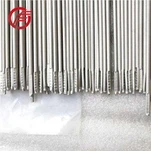


LED grain point measurement and sub-inspection are necessary and important work in the production process of LED products. A probe is used in the process of LED grain point measurement. It is usually tested and sub-inspected according to several key values such as electrical value, brightness, wavelength, ESD, etc., and then the packaging engineering is carried out. Therefore, it is an important process that has a considerable influence on the manufacturing cost in the manufacture of LED. Its main application ranges are:
(1) It is suitable for point measurement of photoelectric characteristics in grain manufacturing of LED.
(2) It is suitable for the point measurement of photoelectric characteristics in semiconductor laser components such as VCSEL, EELD, and DFB grain fabrication.
(3) It is suitable for point measurement of photoelectric characteristics in photosensing components such as Photodiode (PD), Phototransistor (PTR), Schottky diode, and Zener diode grain manufacturing.